 Loading... Please wait...
Categories
Don’t Cross Analog and Digital Grounds Carelessly
Posted on Aug 30th 2025
When designing mixed-signal PCBs that include both analog and digital components, one of the most common pitfalls is mishandling ground planes. At first glance, it may seem intuitive to separate analog and digital grounds completely — but doing so without careful consideration can create more problems than it solves.
Why Grounding Matters
Digital circuits are noisy by nature. High-speed switching generates fast transients that propagate through the ground plane, while analog circuits require a clean, stable reference to measure low-level signals accurately. If analog and digital grounds are tied together haphazardly, that digital noise can leak into sensitive analog paths, degrading performance.
The Right Way to Handle Grounds
-
Use a single, continuous ground plane whenever possible.
Splitting ground planes can cause return current issues and create unexpected impedance paths, leading to crosstalk and noise coupling. -
If you must separate, connect at a single point.
When analog and digital sections require isolation, connect the two grounds at a carefully chosen “star point” to control current return paths. -
Place components strategically.
Keep analog and digital circuits physically separated on the board and route signals so that high-speed digital traces do not cross sensitive analog regions. -
Use proper decoupling and filtering.
Bypass capacitors and ferrite beads can help reduce high-frequency noise transfer between domains.
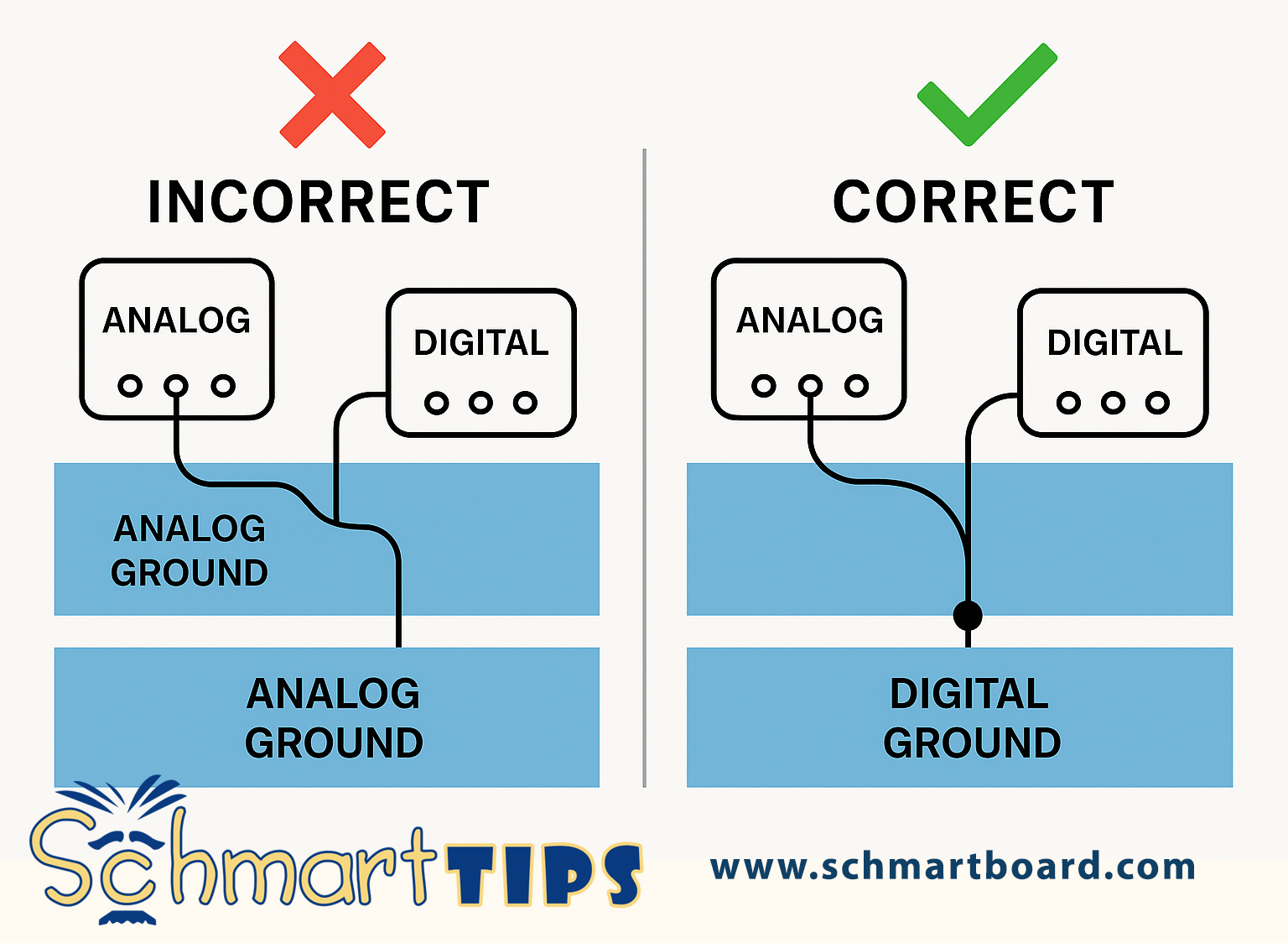
Why the “Incorrect” Side Is Wrong
On the left side of the graphic:
-
The analog and digital grounds are split into two separate planes.
-
However, a signal trace crosses the split, forcing the return current to find an indirect, noisy path.
-
This creates a large ground loop, which:
-
Increases electromagnetic interference (EMI).
-
Causes voltage offsets between analog and digital references.
-
Makes the analog measurements less reliable.
-
Essentially, the split is useless unless return currents are controlled.
Why the “Correct” Side Works
On the right side of the graphic:
-
Analog and digital circuits are still physically separated on the PCB for noise control.
-
However, the two ground planes are connected at a single “star point.”
-
Return currents now follow a short, controlled path, minimizing noise injection.
This approach preserves the quiet environment for analog signals while allowing both systems to share a common ground reference.
Common Mistakes to Avoid
-
Crossing signal traces over ground splits — this forces return currents through unintended paths, creating EMI issues.
-
Placing mixed-signal ICs without considering where their reference grounds connect.
-
Ignoring data sheet recommendations for grounding sensitive components like ADCs, DACs, and RF modules.
Final Thoughts
Good grounding practices are the foundation of robust mixed-signal PCB design. Whether you're working on a hobby project or a production-ready prototype, understanding how return currents behave and controlling where analog and digital grounds meet will save you from signal integrity headaches later.
At Schmartboard, our prototyping boards are designed with best practices in mind, making it easier to experiment without running into common grounding pitfalls.
Recent Posts
- » Do Inspect Solder Joints Under Magnification for Intermittent Issues
- » Don’t Assume Power Supplies Are Perfectly Clean
- » Do Choose the Right PCB Stack-Up Early to Support Signal Integrity
- » Do Route High-Frequency Signals with Controlled Impedance
- » Don’t Overcrowd the Board — Leave Room for Debugging

