 Loading... Please wait...


Categories
Do Choose the Right PCB Stack-Up Early to Support Signal Integrity
Posted on Oct 12th 2025
When designing a printed circuit board (PCB), it’s easy to jump straight into component placement and routing. But before you lay down a single trace, there’s one foundational decision that determines the success of your entire design:
Your PCB stack-up.
The stack-up refers to how the layers of your PCB are arranged — signal layers, power planes, ground planes, and dielectric materials. Choosing the proper stack-up early in the design process is essential for signal integrity, manufacturability, and electromagnetic performance.
Why Stack-Up Matters
High-speed and high-performance circuits rely on controlled impedance and clean return paths. These depend heavily on your stack-up. A poor layer structure can lead to:
-
Signal reflections
-
Crosstalk between traces
-
Increased electromagnetic interference (EMI)
-
Unstable power delivery
-
Difficulty passing compliance testing
But a well-designed stack-up helps:
✅ Maintain signal integrity
✅ Reduce EMI
✅ Control impedance
✅ Enable faster routing
✅ Improve thermal performance
✅ Lower overall PCB cost
Typical PCB Stack-Up Example
Here’s a common 4-layer stack-up used in mixed-signal designs:
| Layer | Purpose |
|---|---|
| Top Layer | Signals |
| Layer 2 | Ground Plane |
| Layer 3 | Power Plane |
| Bottom Layer | Signals |
This type of stack-up provides excellent signal return paths and makes controlled impedance routing easier.
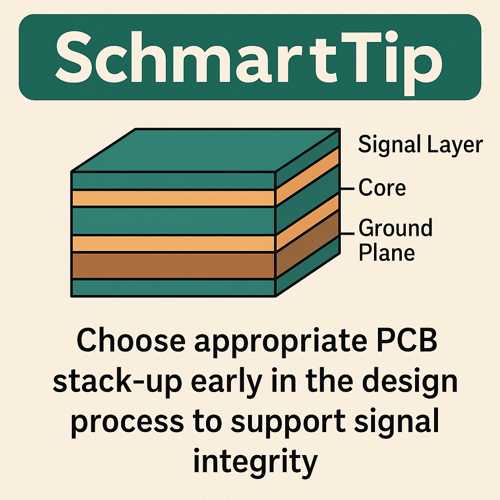
Key Stack-Up Design Tips
When planning your stack-up:
1. Include a solid ground plane
Place a continuous ground layer adjacent to signal layers. This stabilizes impedance and prevents signal noise.
2. Keep power and ground close
Tightly coupled power and ground planes act as built-in decoupling, reducing noise and ripple.
3. Use symmetric layer stacks
Balanced builds minimize bowing or warping during manufacturing.
4. Plan for impedance
Use your stack-up to meet impedance targets like 50Ω single-ended or 100Ω differential.
5. Collaborate with your PCB manufacturer
Fabricators provide standard stack-ups with known dielectric values — use these instead of guessing.
How Schmartboard Helps
At Schmartboard, we understand that stack-up decisions can be overwhelming — especially for engineers and makers who want to move quickly from idea to prototype. Our prototyping boards use professional-grade layouts with solid ground planes and clean routing structures, helping you build reliable circuits without worrying about stack-up problems early on.
Using Schmartboard:
-
Helps prototype high-speed or sensitive circuits reliably.
-
Reduces signal noise during testing.
-
Mimics industry-standard stack-ups, ensuring easier production migration.
Final Thoughts
Your PCB is only as strong as its foundation — and the stack-up is that foundation. Choosing it early isn’t just a best practice; it’s a critical design strategy to ensure clean signals, stable power, and a reliable product.
So before you route that first trace, ask yourself:
✅ Have I defined the stack-up?
✅ Does it support my signal integrity needs?
✅ Will it scale from prototype to production?
Design smarter. Design cleaner. And prototype confidently with Schmartboard.
Recent Posts
- » Do Inspect Solder Joints Under Magnification for Intermittent Issues
- » Don’t Assume Power Supplies Are Perfectly Clean
- » Do Choose the Right PCB Stack-Up Early to Support Signal Integrity
- » Do Route High-Frequency Signals with Controlled Impedance
- » Don’t Overcrowd the Board — Leave Room for Debugging