 Loading... Please wait...
Categories
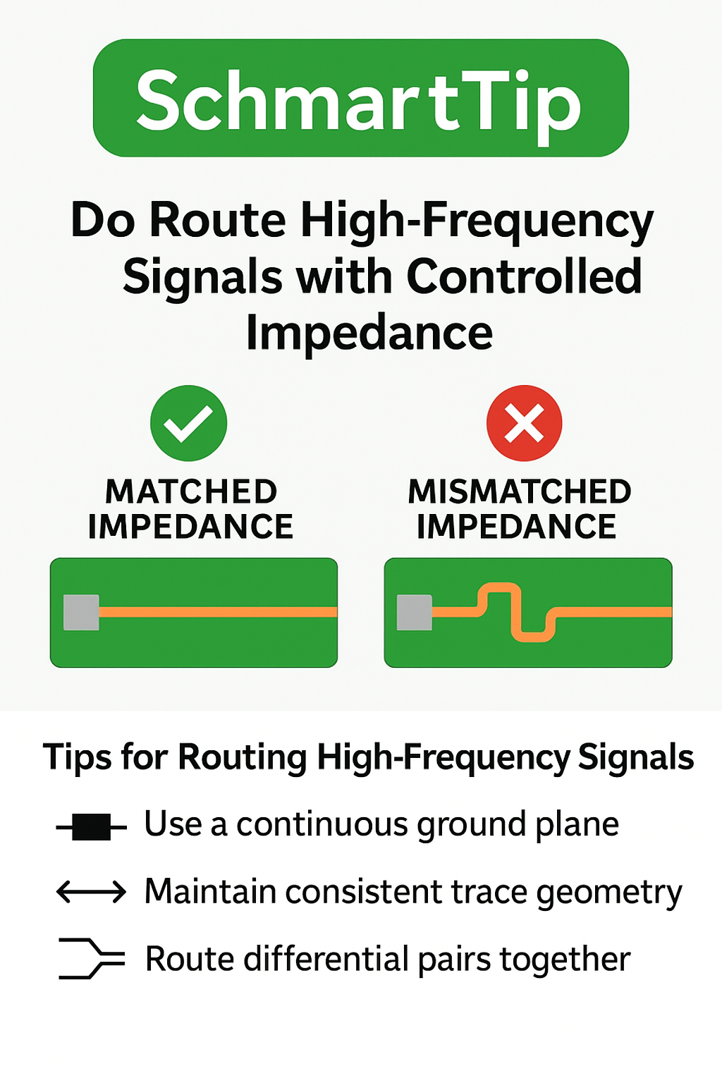
Do Route High-Frequency Signals with Controlled Impedance
Posted by Schmartboard on Oct 7th 2025
When working on high-speed or RF (radio frequency) circuits, your PCB traces are no longer just simple wires — they become transmission lines. And at that point, impedance control is essential for ensuring signal integrity, preventing reflections, and maintaining reliable performance.
If you’re designing for USB, HDMI, Ethernet, DDR memory, or any fast digital interface, you can’t ignore this principle:
Do route high-frequency signals with controlled impedance.
Why Controlled Impedance Matters
At high frequencies (typically above ~50 MHz, but sometimes even lower), a PCB trace’s geometry and surrounding materials start to influence signal behavior.
If the impedance of a trace doesn’t match the device it’s connected to — for example, a 50Ω or 100Ω differential pair — part of the signal will reflect back toward the source, causing distortion, data errors, and EMI issues.
In short:
✅ Matched impedance = clean, stable signal
❌ Mismatched impedance = noise, reflections, and unreliable communication
What Affects PCB Impedance
Several factors determine a trace’s impedance, including:
-
Trace Width and Thickness – Wider traces reduce impedance, while thinner traces increase it.
-
Dielectric Height – The distance between the signal trace and the ground plane strongly influences impedance.
-
PCB Material (Dielectric Constant, or Dk) – FR-4, Rogers, and other materials each affect the signal differently.
-
Reference Plane Placement – A continuous ground plane below the trace helps maintain a consistent impedance.
-
Differential Pair Spacing – For high-speed signals (like USB or Ethernet), the distance between paired traces is critical.
Best Practices for Routing High-Frequency Signals
-
Use a Continuous Ground Plane
This provides a stable reference for return currents and minimizes impedance fluctuations. -
Maintain Consistent Trace Geometry
Don’t vary width or spacing mid-route. Sudden changes can cause signal reflections. -
Route Differential Pairs Together
Keep them the same length, spacing, and layer — and avoid vias when possible. -
Avoid Sharp Corners
Use 45° or curved bends to reduce impedance discontinuities and reflections. -
Use Impedance Calculators or Stackup Tools
PCB design software and online tools (like Saturn PCB or your fabricator’s calculators) can help you design for exact impedance targets. -
Consult Your Fabricator
PCB manufacturers often provide standard stackups with known impedance values — use those to your advantage.
How Schmartboard Helps
At Schmartboard, we make it easier for engineers and hobbyists to prototype and test high-frequency circuits without guesswork. Our boards are designed with proper grounding, clean trace geometry, and reliable material properties — features that align with professional impedance control standards.
When experimenting with RF modules, microcontrollers, or fast digital interfaces, Schmartboard products help you:
-
Prototype cleanly without signal degradation.
-
Maintain short, direct signal paths.
-
Test your design before committing to a production PCB.
With Schmartboard, you can focus on innovation, not layout headaches.
Final Thoughts
As signal speeds climb, impedance control moves from “nice-to-have” to absolutely essential.
Routing high-frequency signals with controlled impedance ensures signal integrity, reduces EMI, and helps your designs perform as intended.
So before you route that next high-speed trace, remember:
It’s not just a wire — it’s a transmission line. Design it that way.
And when you’re ready to test your ideas quickly and confidently, reach for Schmartboard — the smarter way to build, test, and learn high-speed design fundamentals.
Recent Posts
- » Do Inspect Solder Joints Under Magnification for Intermittent Issues
- » Don’t Assume Power Supplies Are Perfectly Clean
- » Do Choose the Right PCB Stack-Up Early to Support Signal Integrity
- » Do Route High-Frequency Signals with Controlled Impedance
- » Don’t Overcrowd the Board — Leave Room for Debugging