 Loading... Please wait...
Categories
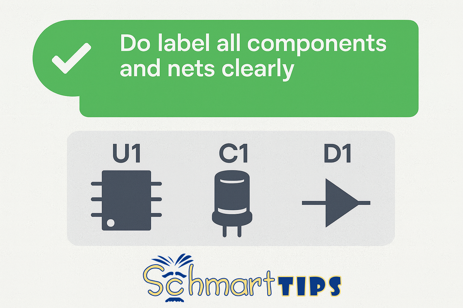
Do Label All Components and Nets Clearly: A Schmartboard Tip
Posted by Schmartboard on Aug 23rd 2025
In the world of electronics design, clarity is everything. Whether you’re prototyping on a breadboard, working on a Schmartboard, or finalizing a PCB for production, one of the most overlooked yet critical steps in the design process is properly labeling your components and nets. This small habit can save you from big headaches later.
Why Labeling Matters
When working with integrated circuits, capacitors, resistors, diodes, and nets (signal paths), it’s easy to think “I’ll remember what connects where.” Unfortunately, as projects grow in complexity, that confidence can quickly turn into confusion.
Proper labeling ensures:
-
Faster Debugging – If something fails, you can quickly locate and test the exact component or connection.
-
Easier Collaboration – Anyone else working on your project (or future you!) can understand the schematic and layout without guesswork.
-
Reduced Errors – Miswiring or misplacing components is far less likely when everything is clearly labeled.
-
Simpler Scaling – If you plan to move from a prototype on a Schmartboard to full PCB production, consistent labeling is essential.
Best Practices for Labeling Components
At Schmartboard, we’ve helped thousands of engineers, makers, and students streamline their design process. Here are a few pro tips to keep your projects organized and error-free:
1. Use Standard Naming Conventions
Follow the common designators:
-
U1, U2, U3 → Integrated circuits
-
R1, R2, R3 → Resistors
-
C1, C2, C3 → Capacitors
-
D1, D2 → Diodes
-
J1, J2 → Jumpers or connectors
This creates a universal language so anyone can pick up your schematic and immediately understand it.
2. Label Nets Clearly
Don’t leave wires unnamed. Give each net a descriptive name based on its function:
-
VCC_5V instead of “Net1”
-
GND_SENSOR instead of “GND2”
-
DATA_TX instead of “Net_A”
On a Schmartboard prototype, this means using consistent labeling from your schematic to your wiring.
3. Match Schematics to Physical Layout
Your labels on paper should match your actual build. When you use Schmartboard prototyping boards, we recommend marking component locations with a fine-tipped marker or adhesive labels. This simple habit makes troubleshooting much easier.
4. Document as You Go
Whether you’re using CAD software or manually wiring a Schmartboard, don’t wait until the end to label things. Documenting connections as you make them saves you time and prevents forgotten details.
How Schmartboard Makes It Easier
Schmartboard products are designed to bridge the gap between schematics and prototypes. Our boards feature:
-
Pre-labeled pads to make component placement intuitive.
-
Prototyping-friendly layouts that match common designators.
-
Integrated soldering guides to keep components secured and organized.
By combining Schmartboard’s smart design with clear labeling, you can confidently take your project from concept to production without losing track of your components or nets.
Final Thoughts
Proper labeling might feel like a small task, but it’s one of the most powerful habits you can develop as a designer. It improves collaboration, simplifies troubleshooting, and accelerates your path from prototype to finished product.
At Schmartboard, our goal is to make electronics easier, smarter, and faster. Labeling your components and nets clearly is a foundational step in achieving that goal.
Schmartboard Tip
“A well-labeled schematic today saves hours of frustration tomorrow.”
Recent Posts
- » Do Inspect Solder Joints Under Magnification for Intermittent Issues
- » Don’t Assume Power Supplies Are Perfectly Clean
- » Do Choose the Right PCB Stack-Up Early to Support Signal Integrity
- » Do Route High-Frequency Signals with Controlled Impedance
- » Don’t Overcrowd the Board — Leave Room for Debugging